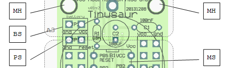
Tutorial 001: Blinking LED
UPDATE: New version of this tutorial is available on the Tutorial 001: Blinking LED x1 page. This is a very simple tutorial on how to make a LED blinking. Since the Tinusaur board is a very standard ATtiny breakout board this could be applied to almost any such other board. The code was tested to work with … Read more