In this post are discussed some of principals used while designing this board.
Size and form factor
The goal of making this board is not to have a smaller or the smallest PCB that runs on ATtiny. The goal is to have a board that could be used for prototyping simple projects as well as fitting reasonable small (or large, depending on the view) circuits on an additional shield board.
Headers
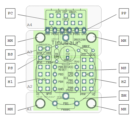
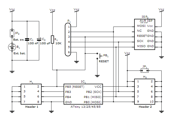
There are 2 header – one 2×4 – H1 and another one 2×5 – H2.
The idea is that all the outer pins are GND while all the inner pins are connected directly to the MCU. The longer header H2 has its top-left pin connected to the Vcc like the 2nd-row one on the left. That gives us one more power source wire.
MCU
This board could work with the smaller Atmel AVR ATtiny controllers such as ATtiny 25/45/85, ATtiny13 as well as most of their variations – as long as they are in DIP-8 case.
Programming
The programming is done through the standard 10-pin ISP connector using any compatible AVR ISP programmer. On the diagram below it is marked as PC.
The connector is placed on the board in such a way so it could be chopped off if not needed and make the board little smaller. The programming probe, marked as PP on the diagram below, has holes that could help in the cutting. In case you need to connect the board to a programmer again at later time you can solder some wires to what’s left of the probe.
Board
Technical parameters: 2 layer board of 0.90×1.40 inches (22.96×35.66 mm).
There are 4 mounting holes marked as MH on the diagram below.
Power
During the development the board could be powered through the ISP programmer.
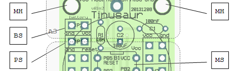
External power source could be connected to the board through a jumper marked as PS on the diagram below.
There is an optional button-cell battery mount on the back of the board, marked as BM on the diagram below. The battery could be switched on and off using the jumper that is marked as BS on the diagram.
Areas
There are 4 areas that a Tinusaur board could be divided to: A1, A2, A3, A4. That is applicable for the actual Tinusaur main board as well as any shield boards one could produce.
A1, the bottom part of the board:
- this is the area where the RESET button is placed on the main board.
- for a shield board that area could be used to put some components and produce a simple circuit.
A2, the mid of the board – heads:
- there are 2 header – one 2×4 and another one 2×5, they are different for a reason.
- on the main board, between the headers, is placed the MCU.
- on a shield board, between the headers, could placed a 8-pin chip or other components.
A3, the top part of the board:
- there are the minimum required components for the MSU to work – 2 capacitors for the power source and one pull-up resistor for the RESET.
- jumper for external power.
- jumper to switch on/off battery.
A4, tip of the board:
- standard ISP programming connector.
Additionally …
A5, the other side of the board:
- there is optional cell-button battery mount.